What is PCB Fabrication? PCB Fabrication is the abbreviated term for printed circuit board production, encompassing the complete process of transforming circuit pattern designs into physical, functional bare PCB boards.
PCB Fabrication falls within the electronics manufacturing sector. With technological advancement, this industry has maintained a state of rapid development. As a vital component within electronic products, PCBs have assumed an increasingly prominent role within the electronics manufacturing field. The knowledge and technologies involved in PCBs—such as electronic components, circuitry, and electronic design—are intrinsically linked to electronics manufacturing.
PCB Fabrication falls under the precision manufacturing sector. It demands exceptionally high manufacturing accuracy; any error may result in the loss of the entire product, making precision its most fundamental requirement. Consequently, the PCB Fabrication sector has attained advanced technical capabilities in processing specification control. This enables the precise production of PCBs in diverse specifications and for varied applications, addressing complex manufacturing demands. Further categorisation distinguishes between rigid PCBs, flexible PCBs, and rigid-flex PCBs, among other types, to meet the requirements of different sectors and products.
The PCB Fabrication process typically encompasses several critical stages: design, pre-fabrication processing, photoplotting, exposure and development, etching, lamination, plating of vias, solder resist/screen printing, post-processing and electrical testing, culminating in final assembly techniques. Each step possesses unique characteristics that directly influence the PCB’s final quality. Every stage requires meticulous design to fulfil the product’s functional requirements and performance metrics.
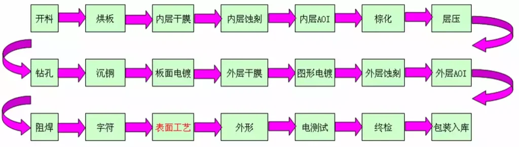
PCB Fabrication Process:
Prototyping and Validation
This stage marks the commencement of PCB Fabrication, aiming to establish product functionality and performance specifications whilst undertaking preliminary layout design and validation.
Schematic and Layout:
Prototype Specification Definition: Engineers preliminarily determine PCB specifications based on product functional requirements, performance metrics, and physical dimensions. This encompasses layer count, component types and quantities, alongside anticipated operating environments.
Layout Planning: Professional PCB design software is employed to plan the arrangement of electronic components. Layout considerations encompass signal flow and electromagnetic compatibility, alongside thermal management, power distribution, and mechanical structure compatibility.
Layout Verification:
Design Rule Checks: Automated tools validate compliance with specific design rules, such as trace width, spacing, and component clearance, ensuring adherence to manufacturing and electrical specifications.
Signal and Thermal Analysis:
Signal integrity analysis is conducted via simulation software to evaluate the transmission quality of high-speed signals on the PCB. Concurrently, thermal analysis ensures the PCB can operate stably under high loads.
Manufacturing Preparation
Following design validation, the manufacturing preparation phase commences, primarily involving material selection and the generation of manufacturing documentation.
Material Selection:
Substrate Material: Substrate material selection requires consideration of electrical, mechanical, thermal properties, and cost. For instance, FR-4 is a common substrate, while PTFE is suitable for high-performance applications due to its high-frequency characteristics.
Copper Foil: Copper foil thickness impacts circuit current-carrying capacity and signal transmission quality. Engineers select appropriate thickness based on current requirements and signal characteristics.
Manufacturing Documentation Generation:
Plotter Files: Design schematics are converted into plotter files, a critical step directly impacting the precision of subsequent photolithography processes.
Drilling Data: The accuracy of drilling data directly affects component mounting and circuit interconnections. Files must precisely define the position, dimensions, and depth of each hole.
Internal Layer Fabrication
This stage constitutes a pivotal step in multilayer PCB Fabrication, involving the precise formation of circuit patterns on internal copper foil layers.
Copper Foil Laminating: Copper foil is meticulously laminated onto the substrate material; any air bubbles or defects may compromise product quality and reliability.
Pattern Transfer: Circuit patterns are transferred onto the copper foil using high-precision photolithography equipment. Exposure time and light intensity must be precisely controlled to ensure pattern clarity and accuracy.
Etching Process: Chemical etching requires precise control of etching duration to ensure uniform copper removal, preventing over- or under-etching.
Cleaning and Drying: Thorough cleaning removes photoresist and etchant residues to prevent contamination in subsequent processes. Drying ensures the PCB is completely dry, avoiding moisture interference with lamination.
Outer Layer Fabrication
Outer layer fabrication involves laminating inner layers together and preparing for outer layer circuitry.
Prepreg Laying: Prepregs must be precisely aligned with the inner layer copper patterns to guarantee accurate multi-layer PCB registration.
Lamination Process: During lamination, temperature and pressure must be controlled to ensure robust bonding between layers while preventing material damage.
Drilling Process: Drilling demands precise positioning and dimensions, alongside attention to hole wall integrity to facilitate subsequent plating operations.
Outer Layer Pattern Formation
This stage mirrors inner layer fabrication but involves etching circuit patterns onto the outer copper layers.
Outer Layer Copper Fabrication: Precise pattern transfer and etching processes are required to form the outer layer circuits.
Cleaning and Drying: Cleaning and drying steps are crucial for removing residues from the etching process and preparing for subsequent via plating and surface finishing.
Hole Metallisation and Surface Treatment
This stage aims to establish electrical connections within multilayer PCBs and protect the circuit board.
Via Formation: Via formation is pivotal for establishing electrical connections between inner and outer layers of multilayer PCBs. Chemical copper plating or conductive paste filling techniques ensure conductive properties of the via walls.
Surface Finishing: Surface finishing enhances the PCB’s corrosion resistance and improves solderability. Selecting appropriate surface finishing techniques, such as gold plating, tin plating, or OSP, requires balancing the product’s application environment and cost-effectiveness.
Component Assembly
The assembly stage involves mounting electronic components onto the PCB.
Component Placement: Automated placement machines enhance speed and precision, with placement quality directly impacting soldering outcomes and product reliability.
Soldering Process: Soldering techniques are selected based on component types and PCB design requirements. Methods including lead-free soldering, wave soldering, and reflow soldering each possess distinct advantages and limitations.
Testing and Inspection
This stage verifies the PCB’s functionality and performance to ensure compliance with design specifications.
Functional Testing: Validates whether the PCB operates correctly as designed. Automated test equipment rapidly detects circuit functionality issues.
Visual Inspection: Identifies visible defects on the PCB, such as solder joint flaws, component misalignment, or silk screen errors.
Performance Testing: Includes signal integrity testing, thermal performance testing, and electromagnetic compatibility testing to ensure the PCB maintains high performance under various operating conditions.
Inspection and Packaging
This constitutes the final stage of PCB Fabrication, ensuring the product meets all quality standards and is properly delivered.
Quality Inspection: The final step to ensure the PCB meets all specification requirements. Typically involves a comprehensive check of the PCB’s dimensions, appearance, and performance.
Packaging: Appropriate packaging safeguards PCBs against damage during transit and storage, ensuring products arrive at customers in optimal condition.
Assessing PCB Design Manufacturability Prior to Production
Conduct a design review, thoroughly examining circuit board design documentation including schematics, PCB layouts, and routing. Verify compliance with industry standards such as IPC specifications to ensure production feasibility.
Examine the PCB layout and routing. Ensure critical components are positioned rationally to prevent signal interference and crosstalk. Trace widths and spacing must meet the manufacturer’s process specifications, while special routing features (e.g., blind vias, buried vias) require confirmation of technical feasibility.
Consider component selection and layout rationality. Opt for readily available standard components, avoiding rare parts to reduce production costs and shorten lead times. Simultaneously, arrange components on the PCB Fabrication automated placement while ensuring ease of maintenance and repair.