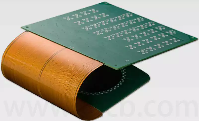
Rigid flexible PCB, in essence, are printed circuit boards formed by precisely combining flexible printed circuits (FPC) with rigid printed circuit boards (PCB) through processes such as lamination. This type of board not only combines the flexibility of FPC with the rigidity of PCB but also possesses a range of unique characteristics, making it widely used in the production of various electronic products.
Common Structures of Rigid Flexible PCB
- Single-sided structure: One side comprises a rigid board, the other a flexible board, connected via plated-through holes (PTH).
- Double-sided structure: Rigid and flexible boards are positioned on opposite sides, electrically interconnected through conductive vias.
- Hybrid structure: Integrates multiple rigid and flexible zones onto a single board, enabling complex multi-layer routing designs as required.
- Multi-layer laminated structure: A complex combination of multiple rigid and flexible layers, suitable for high-end electronic products.
The manufacturing process of rigid flexible PCB combines the dual characteristics of FPC and PCB. Consequently, the production workflow requires not only FPC manufacturing equipment but also PCB production machinery to ensure the perfect balance of flexibility and rigidity in the final product.
Process Flow
- Design and Pre-preparation
Design Phase: Circuit design utilises CAD software to ensure precise alignment between rigid and flexible sections.
Material Selection: Appropriate substrates such as PI (polyimide) or FR4 are chosen based on product requirements.
Conductive Layer Fabrication: Conductive patterns are formed via photolithography. - Inner Layer Pattern Formation
Inner Layer Transfer: Transfer design patterns onto copper-clad laminates using methods including photolithography or Laser Direct Imaging (LDI).
Etching Process: Remove excess copper chemically to form the required circuit patterns. - Laminating
Rigid Laminating: Bond pre-treated inner layers with other rigid substrates.
Flexible Laminating: Combining flexible substrates with conductive layers, typically employing hot-pressing techniques.
Key Laminating Control Points:
1) Regulate the flow of No-Flow PP to prevent excessive resin flow.
2) Due to No-Flow PP windowing causing pressure loss during lamination, use conforming pads and release film to equalise pressure across varying elevations.
3) Pre-lamination baking of both rigid outer and flexible inner layers is mandatory. This eliminates latent thermal stresses, ensuring metallisation quality and dimensional stability.
4) Select appropriate cushioning materials. Ideal cushioning should exhibit excellent conformability, low flow characteristics, and no shrinkage during thermal cycling to prevent blistering and deformation of flexible substrates during lamination.
5) Post-lamination quality inspection: Examine the board’s appearance for defects such as delamination, oxidation, or resin overflow. Conduct peel strength testing concurrently. - Drilling and Copper Plating
Mechanical drilling: Perform mechanical drilling at designated locations to facilitate subsequent component mounting or interlayer connections.
Copper Plating: Apply a copper layer to the hole walls via chemical or electrolytic plating to ensure reliable electrical connections. - Outer Layer Pattern Formation and Etching
Outer Layer Fabrication: Similar to inner layer production, outer circuits are formed through pattern transfer and etching.
Flexible Circuit Fabrication: Create circuit patterns on flexible substrates while preserving the bending properties of flexible areas. - Rigid flexible PCB Assembly
Lamination Process: Precisely align and bond the fabricated flexible circuit to the rigid substrate. Common methods include hot-press lamination and adhesive bonding. - Surface Finishing
Pad Treatment: Process exposed copper surfaces with techniques such as gold plating, OSP (Organic Solderability Preservative), or tin spraying to enhance solderability and prevent oxidation. - Testing and Quality Control
Electrical Testing: Conduct circuit continuity checks to ensure no open circuits or short circuits exist.
Functional Testing: Perform functional assessments on assembled boards to validate overall circuit performance.
Quality Inspection: Examine appearance, dimensions, layer-to-layer alignment, etc., to ensure product quality meets standards. - Assembly and Finished Product
Component Mounting: Install components via SMT (Surface Mount Technology) or THT (Through-Hole Technology).
Final Testing: Conduct comprehensive functional testing to ensure the product meets all technical requirements prior to delivery.
Core Advantages of Rigid Flexible PCB
High-Density Integration
Through multi-layer design and micro-via technology, rigid flexible pcb achieves greater routing density. This high-density integration capability enables them to support more complex circuit designs, meeting the demands for high performance and miniaturisation in premium electronic products. For instance, Hengtianyi’s rigid-flex boards are utilised in smartphones to connect camera modules and foldable screens, thereby enhancing device performance and user experience.
Superior Mechanical Properties
Combining the strength of rigid boards with the flexibility of flexible boards, rigid flexible pcb withstand vibration, impact, and repeated bending, making them suitable for demanding environments. Within automotive electronics, for instance, Hengtianyi’s rigid-flex boards are extensively deployed in in-vehicle displays, sensors, and battery management systems, ensuring stable operation under high-temperature, high-humidity, and vibration-prone conditions.
Signal Integrity
Rigid flexible pcb minimise reliance on traditional connectors (such as cables and sockets), reducing signal attenuation and electromagnetic interference while enhancing transmission stability and speed. This advantage is particularly pronounced in 5G communication equipment, where Hengtianyi’s boards facilitate high-speed signal transmission, guaranteeing efficient and stable data transfer.
Lightweight Design
Compared to conventional rigid boards, rigid flexible pcb offers reduced weight, making them particularly suitable for weight-sensitive applications. For instance, in drones and wearable devices, Hengtianyi’s rigid-flex boards enable slimmer, more portable designs through their lightweight construction.
High Reliability
Rigid flexible pcbs minimise connection points and solder joints, reducing failure rates while enhancing overall equipment reliability through integrated design. This high reliability is particularly crucial in aerospace and medical devices. Heng Tian Yi’s flex-rigid boards are extensively used in satellite communication equipment and endoscopes, ensuring stable operation under extreme conditions.
Application Domains of Rigid Flexible pcb:
- Industrial Applications: Spanning industrial, military, and medical sectors. Products in these fields demand rigid flexible pcb with high reliability, precision, low impedance/loss, complete signal transmission quality, and durability. Due to complex manufacturing processes and low production volumes, fabrication costs remain elevated.
- Mobile phones: Common applications within mobile phones include hinge mechanisms for foldable devices, imaging modules, keypads, and RF Q modules.
- Consumer electronics: Most notably, rigid flexible pcbs used in digital still cameras (DSCs) and digital video cameras (DV). Performance-wise, these boards enable three-dimensional connections between rigid PCBs and components. They increase total PCB footprint at equivalent circuit density, enhancing circuit capacity while reducing signal transmission constraints at connection points and minimising assembly error rates. Structurally, their lightweight, thin profile facilitates flexible routing, substantially aiding compact design and weight reduction.
- Automotive: Common applications include buttons connecting to the mainboard on steering wheels, connections for in-vehicle video systems screens and control panels, operational connections for audio or function keys on side doors, reversing radar imaging systems, sensors, in-vehicle communication systems, satellite navigation, boards connecting rear seat control panels and front-end controllers, and external detection systems.
AiBiPCB rigid flexible pcb offers flexible 1-8 layer configurations to meet diverse application requirements. Copper thickness options range from 1/3 oz to 1 oz to accommodate varying design specifications. For critical parameters like minimum line width and spacing, AiBiPCB provides 0.07mm (0.5 oz), 0.10mm (1 oz), and 0.15mm (2 oz) options, ensuring high-precision circuit fabrication. Furthermore, the maximum board size of 230 x 500mm provides ample fabrication space. AiBiPCB excels in drilling processes, achieving minimum hole sizes of 0.15mm (mechanical drilling) and 0.1mm (laser drilling) to meet diverse requirements. Concurrently, a 6:1 board thickness to aperture ratio and 0.5μm thick gold plating further guarantee product stability and reliability.